
We know that MOSFETs are voltage controlled devices. Unlike bipolar transistors, MOSFETs only need to control the gate voltage to exceed their turn-on threshold voltage for conduction, without the need for gate current. So essentially, there is no need to connect any resistors in series on the gate of the MOS transistor.
For a regular bipolar transistor, it is a current control device. Its base series resistance is designed to limit the magnitude of the base current, otherwise for the driving signal source, the base of the transistor to ground is equivalent to a diode, which will affect the preceding driving circuit.
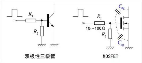
MOS transistors, due to their gate being insulated from the drain and source, do not require a series resistor on the gate for current limiting.
On the contrary, considering the parasitic capacitance present at the gate of the MOS transistor, in order to accelerate the conduction and cutoff speed of the MOS transistor and reduce the losses during the conduction and cutoff process, the equivalent resistance on its gate should be as small as possible.
However, in many practical MOS transistor circuits, the resistor connected in series on the gate of the MOS transistor is almost ubiquitous. It seems that everyone has forgotten that the existence of this resistor will prolong the conduction and cutoff time of the MOS transistor, increasing unnecessary losses.
Why do some circuits still have this resistor placed in front of the gate of the MOS transistor, and what is its purpose?
Firstly, it is important to clarify a concept that analog circuits are not software programming or non-zero, but rather a continuous process of change. Neither the voltage on the capacitor nor the current on the inductor can suddenly change, otherwise catastrophic consequences will occur. The steeper the rising and falling edges, the better. Sometimes, in the design, some resistors are intentionally added to make the rising and falling edges smoother to protect the components.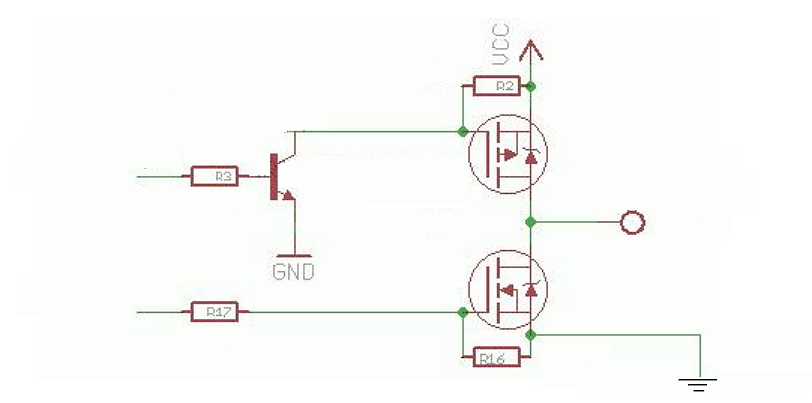
In the above circuit, resistor R17 has three functions: first, to prevent oscillation; second, to reduce the peak charging current of the gate; and third, to protect the D-S terminal of the MOS transistor from breakdown.
Firstly, let's take a look at the first point. Generally, the I/O output ports of microcontrollers carry some stray inductance, which may cause LC oscillation with the gate capacitance in the event of a sudden voltage change. When R17 is connected in series between them, the damping can be increased and the oscillation effect can be reduced.
Secondly, when the gate voltage is raised, the gate capacitor will first be charged, and the peak charging current will exceed the I/O output capacity of the microcontroller. After connecting R17 in series, the charging time can be slowed down to reduce the gate charging current.
Thirdly, when the gate is turned off, the D-S electrode of the MOS transistor changes from a conducting state to a cut-off state, and the drain source voltage VDS rapidly increases. If it is too high, it will break down the device. Therefore, adding R17 can slowly discharge the gate capacitance without causing device breakdown.
What is the required value for this resistor?
This usually needs to be determined based on the actual situation, but we can roughly judge the impact of the value based on the following experiment.
The MOS transistor gate in the following circuit is connected in series with resistor R3, and its drain load is an inductive load, which also includes line distributed inductance.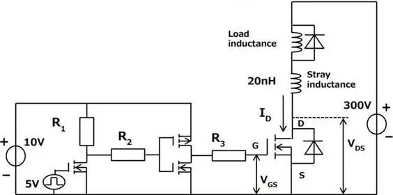 In the experiment, simulation experiments were conducted on R3 with 1 ohm, 10 ohms, and 50 ohms respectively. When R3 is 1 ohm, a high-frequency oscillation signal can be seen on the output voltage Vds.
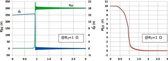 When R3 increases to 10 ohms, the high-frequency oscillation signal of the output Vds is significantly attenuated.
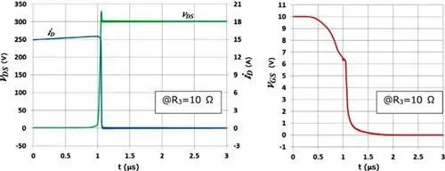 When R3 increases to 50 ohms, the rising edge of Vds becomes relatively slow. On its gate voltage, there is also a noticeable step caused by the Miller capacitance effect between the drain and gate. At this point, the power consumption of the corresponding MOS transistor greatly increases.
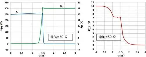 Based on the experimental results above, the resistance connected in series on the gate of the MOS transistor needs to be determined according to the specific MOS transistor and circuit distribution of stray inductance. If its value is too small, it will cause output ringing, and if it is too large, it will increase the switching transition time of the MOS transistor, thereby increasing power consumption.
Hot
-
In depth analysis of the working principle of MOS transistor
2025-05-19
-
Comprehensive Analysis and Recommendation of MOS Tube Brands
2025-05-19
-
A Comprehensive Guide to MOS Tube Selection
2025-05-19
-
The vast prospects and development trends of the MOS transistor market
2025-05-19
-
Comprehensive analysis of MOS transistor performance parameters
2025-05-19
-
In depth Analysis of MOS Tube Price Trends
2025-05-19
-
A comprehensive guide for troubleshooting MOS transistor faults
2025-05-19
-
Analysis of the Growth Trend of Trench Mosfet Market
2025-05-19
-
Analysis of MOSFET Working Principle
2025-05-19
-
A Comprehensive Guide to MOS Tube Selection
2025-05-19

Follow Mingkexin Semiconductor